
会社紹介
1962年の創業以来、当社は「技術で社会課題を解決する」という姿勢のもと、時代の一歩先を読み、電子部品や機能性材料の革新を重ねてきました。その道のりは、目の前の課題に向き合うだけではなく、「次に来る変化」への挑戦の連続でした。私たちが一貫して大切にしてきたのは「お客さまと一緒に明日を思い描き、課題を一つひとつ解決していく」という姿勢です。
私たちはこれからも、「Empower Evolution. つなごう、テクノロジーの進化を。」というパーパスのもと、お客さまとともに、未来の価値創造につながる製品とソリューションを生み出し続けます。

経営理念
「Integrity 誠心誠意・真摯であれ」
わたしたちは、知的で卓越した当社独自の技術でお客さまのニーズ、課題をかしこく、機敏に解決し、お客さまの期待を超える価値を一人ひとりの社員が誠心誠意、真摯に創造します。
企業ビジョン
「 Value Matters 今までなかったものを。世界の価値になるものを。」
わたしたちは、世の中にない新しい価値を提供しつづけ、人間社会と地球環境の豊かさと質の向上に貢献します。そのために価値を創る人をつくることが使命であり、目指すべき企業の姿であると考えています。
デクセリアルズの魅力はココ ‼
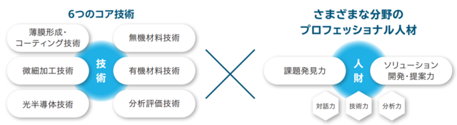
高付加価値創出の源泉であるマテリアリティ「技術」と「人財」
当社のビジネスモデルの根幹にあり、高付加価値創出の源泉となっているのは、マテリアリ
ティである「技術」と「人財」です。社内に蓄積された「薄膜形成・コーティング技術」「微細加工技術」「光半導体技術」「無機材料技術」「有機材料技術」「分析評価技術」の6つのコア技術と、それらを組み合わせて課題解決を実行する多様なプロフェッショナル人材が、製品の競争力を支えています。営業・エンジニアがそれぞれの知見を持ち寄り、連携しながらお客さまと直接対話を行い、課題の本質に迫る提案活動を展開しています。
【世界シェアNo.1】
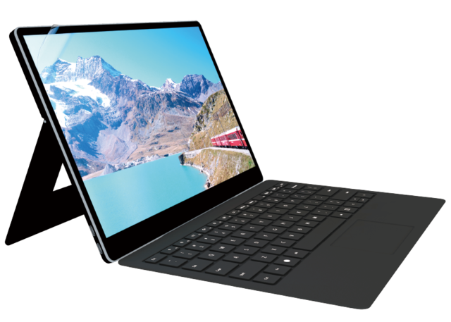
当社の製品は、スマートフォンをはじめノートPCやタブレットPC、薄型テレビなど、みなさんの身近にあるものにも多く使われており、ニッチな市場で高い世界シェアを誇ります。
【主力製品と使用用途】
・異方性導電膜 (ACF):スマートフォン、ノートPC、車載ディスプレイなど
・反射防止フィルム:ノートPC、車載ディスプレイなど
・セルフコントロールプロテクター(SCP):ノートPC、スマートフォン、 コードレス掃除機、電動工具、電動バイク、ドローンなど
・光学弾性樹脂(SVR):タブレットPC、スマートフォン、車載ディスプレイなど
*エンジニア向け技術情報サイト*
デクセリアルズがこれまで培ってきた経験やノウハウを紹介するブログです。
募集ポジションに関連する製品、最新の技術情報を紹介しています!
↓ こちらより、ぜひご覧ください ↓
https://techtimes.dexerials.jp/

※1 株式会社富士キメラ総研発行「2025ディスプレイ関連市場の現状と将来展望」同調査レポート上の市場区分:ACF(大型および中小型ACFの合計)で世界シェア74.0%。
※2 株式会社富士キメラ総研発行「2025ディスプレイ関連市場の現状と将来展望」同調査レポート上の市場区分:表面処理フィルム(ドライコート)で世界シェア92.8%。
※ 株式会社富士キメラ総研発行「2025ディスプレイ関連市場の現状と将来展望」同調査レポート上の市場区分:OCRで世界シェア54.7%。光学弾性樹脂(SVR)は、光学用透明接着剤の当社製品名です。
価値を創る人を創る(社風・風土)
デクセリアルズの魅力のもう一つは、個人の自主性や積極性を大切にし、常に新しいことをやっていこうとする社風です。その根幹にあるのはまさに「人」です。当社は、「価値を創る人を創る」ため、人材育成の活動に力を入れています。自らの可能性を信じ、自ら考えて新しいことに挑戦してみたい方が、デクセリアルズで活躍できる人です。
Position Background
To strengthen our technological capabilities in the Photonics domain, we are seeking a professional with expertise in Parallel Optical Interlink to lead global technology strategy development across Photonics and Semiconductor fields.
You will analyze customer challenges, translate them into target specifications for material and process development, and drive development initiatives. The role also involves technical discussions in English with global partners and potential customers.
Job Description
- Core Technical Expertise
- Optical Communication System Design
- Experience with link budget calculations and modeling of link for simulation.
- Experience with analysis for degradation of optical link and research for compensation.
- Experience defining required performance on optical devices and components.
- Understanding modulation method and demodulation algorithm.
- Chip Architecture for Optical I/O
- Experience defining architecture for optical engines integrated with ASICs or SoCs.
- Understanding of co-packaged optics and chiplet-based designs for high-bandwidth interconnects.
- PHY Design
- Deep knowledge of high-speed SerDes, PAM4 signaling, and optical PHY layer design.
- Familiarity with clock-data recovery (CDR), equalization, and link training for optical channels.
- Parallel Optical Interconnect
- Expertise in multi-lane optical interfaces (e.g., 400G/800G Ethernet, InfiniBand).
- Knowledge of optical modulation formats and encoding schemes.
- Optical Communication System Design
- Required Experience
- PoC for Novel Optical Network Architecture
- Experience with implementation model design.
- Experience prototyping for transmitter, receiver and link media and system performance evaluation.
- Integration & Packaging
- Experience with electrical-optical co-design for chip-to-optical engine integration.
- Understanding of thermal management and mechanical constraints for optical engines in advanced packaging (e.g., 2.5D/3D IC, silicon interposer).
- Experience with RF modeling in optical communication systems.
- Understanding RF degradation factor on link and devices.
- Modeling & Simulation
- Proficiency in signal integrity (SI) and power integrity (PI) analysis for high-speed optical PHY.
- Familiarity with simulation tools: Cadence, Synopsys, Ansys HFSS, Lumerical for photonic modeling.
- Validation & Testing
- Hands-on experience with optical PHY bring-up, BER testing, and compliance validation.
- Knowledge of IEEE and OIF standards for optical interconnects.
- Experience with requirement analysis for conformance on the technical standard.
- Collaboration
- Ability to work across ASIC design, packaging, and optical component teams.
- Strong documentation and communication skills for architecture specs and design reviews.
- Industry & Standards
- Familiarity with CPO (Co-Packaged Optics), PCIe, Ethernet, and InfiniBand standards.
- Awareness of roadmap trends in optical I/O for AI/HPC systems.
- Experience making contributions for standardization.
- PHY design tools
- Familiarity on the tool for architecture stage, and have breath knowledge on the tools for other design stages.
- Design Stage and Tools
- Architecture: MATLAB/Simulink (system modeling), SystemVerilog/VHDL (RTL architecture)
- Circuit Design: Cadence Virtuoso, Synopsys Custom Compiler, Mentor Calibre (DRC/LVS)
- Simulation: Cadence Sigrity (SI/PI), Keysight ADS, Ansys HFSS, Lumerical, Zemax
- Verification: Cadence Xcelium, Synopsys VCS, IBIS-AMI models for compliance
- Testing & Validation: Lab instruments: Keysight Oscilloscopes, BERTs, Optical Power Meters, Components Analyzer, AWG
- PoC for Novel Optical Network Architecture
| 職種 / 募集ポジション | 【FY26_73E】Optical Engine Chip Architecture and PHY Design Engineer for POI |
|---|---|
| 雇用形態 | 正社員 |
| 契約期間 | Full-time Employee |
| 給与 |
|
| 勤務地 | Tokyo Office, Tochigi Headquarters, or Tagajo Site—depending on your preference, while utilizing hybrid work. The final work location will be discussed during the interview process. |
| 勤務時間 | Working Hours: 9:00 – 17:45 Break: 45 minutes *In case of the Tokyo Office as the primary location. *Working conditions may vary depending on each location. |
| 休日 | - Two days off per week (Saturdays, Sundays, national holidays, and year-end/New Year holidays) - Paid leave: 17 to 24 days per year (granted from the date of employment) - Annual holidays: 128 days |
| 福利厚生 | - Retirement benefit system - Company-leased housing program (subject to eligibility criteria) - Stock compensation plan (J-ESOP) - Benefit Station (employee benefits program) |
| 加入保険 | - Health insurance - Workers’ compensation insurance - Employment insurance - Employees’ pension insurance |
| 受動喫煙対策 | - No smoking allowed indoors |
| Work style | Flexible Working Hours (Flextime System) Core Time: 10:00 AM – 2:45 PM *Working hours and core time may vary depending on the location. Remote Work Policy This position primarily follows a remote work style. We have introduced a remote work system to support diverse work styles and enhance productivity, allowing employees to work flexibly based on the nature of their duties and individual suitability. |
| Scope of Changes in Job Responsibilitie | Scope of Changes in Job Responsibilities: All duties as determined by the company |
| 会社名 | デクセリアルズ株式会社 |
|---|---|
| 設立 | 2012年6月20日(平成24年) |
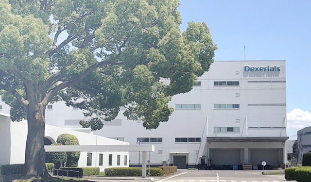
| 本社所在地 | 〒323-0194 栃木県下野市下坪山1724 |
| 資本金 | 【資本金】16,262百万円(2025年3月31日現在) |
| 従業員数 | 1,888名(2025年3月31日現在)※連結ベース |
| 代表取締役社長 | 新家 由久 (しんや よしひさ) |
| 事業内容 | 電子部品、接合材料、光学材料などの開発・製造・販売 |
| 国内事業所 | 本社・栃木事業所、鹿沼事業所、多賀城事業所、東京オフィス、西日本オフィス |
| 国内連結子会社 | デクセリアルズ フォトニクス ソリューションズ株式会社 |
| 海外連結子会社 | Dexerials America Corporation Dexerials Europe B.V. Dexerials (Suzhou) Co., Ltd. Dexerials (Shanghai) Corporation Dexerials Taiwan Corporation Dexerials Korea Corporation Dexerials Singapore Pte. Ltd. |